Nova Metrion®: Analyzing Materials Composition of Complex Stacks
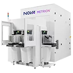
Nova Metrion® directly measures the composition of wafer materials using Secondary Ion Mass Spectrometry (SIMS). Metrion performs SIMS measurements in-line on full 300mm product wafers with complex film stacks for both logic and memory devices.
Performing these measurements in the semiconductor fab, rather than in a cost-and-time intensive laboratory setting, provides faster results, which reduces scrap and improves yield.
First, what is the Nova Metrion®?
The Metrion® is a SIMS tool. SIMS stands for Secondary Ion Mass Spectrometry, a technique widely used in the semiconductor industry to study material composition and depth profiling of semiconductor wafers at the atomic level. To accomplish this feat Metrion determines the concentration of various chemical species vs. distance from the surface of an IC wafer film by sputtering the surface of the wafer, capturing and analyzing the secondary ions.
Conventionally, SIMS equipment has only been available in metrology laboratories that specialize in measuring and characterizing semiconductor devices. In keeping with Nova’s ‘lab to fab’ philosophy, the Nova Metrion® has been intentionally designed to be used in-line in high-volume manufacturing (HVM).
Let’s examine the Metrion SIMS process in more detail.
Metrion SIMS uses an oxygen primary ion beam to sputter a small area on the surface of a silicon wafer. As this primary ion beam sputters through the material on the wafer film, secondary ions are ejected from the surface and are collected and analyzed by a mass spectrometer, which sorts the ions based on tiny differences in their weight. The Metrion’s mass spectrometer utilizes multiple detectors to sort the ions, and the raw data is displayed in a compositional profile showing counts of the secondary ions versus the time frame in which they are detected. Using film analysis software that is built into the Metrion process recipes, the data is quantified, converting counts into concentration and collection time into depth for each measured species.
Another key feature of Metrion is the ability to create maps of entire 300mm wafers with as few as 5 measurement points. These wafer contour maps provide a useful visual representation of within-wafer and wafer-to-wafer uniformity differences.
The numerical data from Metrion is collected and automatically uploaded to the factory host computer where it can be used by fab technical personnel to tune their semiconductor manufacturing processes through a complex mathematical technique called Statistical Process Control. This technique can generate insights that allow users to optimize costs, time, and product yield. By using Metrion as a prevention-based real-time quality control measure, fab personnel can detect trends or changes in their manufacturing process before these result in non-conforming products or scrap.
Why is semiconductor material composition so important?
As the requirements for modern electronic equipment become more complex, semiconductor chips and therefore the films built onto silicon wafers must become more complex as well. Two important types of semiconductors that vary significantly in composition and structure are logic semiconductors (used in data processing) and memory semiconductors (used in data storage). SIMS measurements performed by Metrion can help identify problems with both logic and memory production processes.
Let’s review how Metrion treats both logic and memory structures built onto wafers.
Logic structures for data processing are challenging to implement on silicon. In particular, the uniformity of the SiGe epitaxial layer is critical (epitaxy is the deposition of a thin layer of single-crystal material, in this case, a compound of silicon and germanium onto the surface of a silicon wafer). Besides SiGe epitaxy and residue control, other semiconductor composition priorities for logic chips include the precise control of dopant concentration, reactor matching, and process excursion prevention.
Semiconductor memory structures have generated significant manufacturer interest to control contamination and identify unwanted chemical residues that could reduce yield. Here, the power of SIMS to detect contamination throughout the entire device, and not just at the surface, is key. Other important SIMS functions include semiconductor material composition and thickness measurements, to improve device function.
By looking at potential diffusion, Metrion users can anticipate problems with barrier layers and source/ drain function. The deposition uniformity within wafers and from wafer to wafer is also important because this affects downstream fabrication processes. Insights in these areas provided by SIMS help to improve device performance, reduce scrap, and increase yield.
These are the main advantages of SIMS, which is used widely in metrology labs. However, lab SIMS turnaround time is too long, meaning that the data coming from the lab SIMS measurements takes too long to translate into manufacturing process control improvements, which puts many wafers at risk. Let’s look at this in more detail.
For a lab SIMS service provider, turnaround on wafer measurements can take up to two weeks. For an in-house metrology lab at a semiconductor production facility turnaround could be as short as one day, depending on the number of samples to be measured. However, time-to-results at such a producer lab could suffer if the production team required a quick result. Also, if the producer lab tool goes down, SIMS results could take months to obtain. One solution is to integrate a SIMS tool such as Metrion directly into the semiconductor production line, something it would be impossible to do with a lab tool.
What is the value of inline SIMS?
Laboratory SIMS systems only measure coupons, not full wafers. Wafers must be broken into coupons resulting in scrap. A single point is measured on each coupon. A SIMS expert is required to manually set up each measurement and to analyze the data point by point. This whole process can take days (or weeks as just discussed).
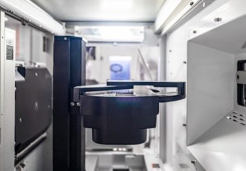
Nova Metrion®, on the other hand, measures whole wafers and is fully automated. Metrion fits seamlessly into the production line, accepting wafers from the fab’s automated transport system, loading them into the Metrion measurement chamber, measuring the wafers, providing full profile data and wafer mapping, and automatically uploading the data to the factory host. All this can be done within minutes. The real advantage of an inline Metrion SIMS system, then, is that the shorter time to data results in tighter process control and improved yield.
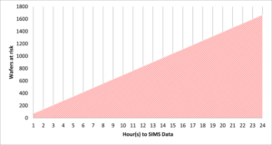
Figure 2 illustrates this point. In a fab with 50,000 wafer starts per month, and a turnaround time for SIMS data of 2 hours, less than 200 valuable wafers will be placed at risk. But if it takes 24 hours to get the SIMS data back from a lab, the number of wafers at risk increases dramatically to 1600. The key point here is that the faster the time to obtain results with Metrion SIMS the more wafers are saved and therefore more money is saved by improving yield.

Figure 1: Wafers at Risk by Hour for 50K Wafer Starts per Month (WSPM)
Not all the wafers have to be scrapped, so let’s imagine a scenario where there is a 3% yield loss due to some problem in the manufacturing process and, further, that this problem is identified by SIMS.
How much would a 3% increase in yield save a fab in one day? Would it save the fab $500, $5,000 or $50,000? (our assumptions are that the fab has 50,000 wafer starts per month and the cost per wafer is $1,000) The answer is that a 3% yield increase could save a fab $7,500 in a single day, a significant amount.
Now let’s imagine that a catastrophic event occurs where all of the wafers at a certain process step are lost, or if 50% of the wafers in a deposition step are lost. That’s going to have a huge financial impact.
Why can’t these savings be achieved by inline metrology today?
There are in-line solutions available, such as LEXES (Low energy Electron Induced X-ray Emission Spectrometry), Ellipsometry, 4-point probe, and XRD (X-Ray Defraction). But these techniques have to be correlated. In other words, no single metrology option exists that will provide a comprehensive picture of what is happening on the wafer.
Nova Metrion® can replace these in-line metrology options because it performs direct measurements of material composition through the entire wafer stack. Metrion also produces full wafer maps of thickness and uniformity based on several points across a wafer. Additionally, the data is automatically uploaded to the factory host for statistical process control.
What makes Nova Metrion® unique?
The Nova Metrion® includes several key features that make it well-suited for high-volume manufacturing. For example, Metrion uses an oxygen ion beam, which is fast, contamination-free, and safe for use in production.
Metrion uses multiple ion detectors, which enable multiple chemical species to be measured simultaneously. It also delivers superior depth resolution and higher data density.
Additionally, Metrion utilizes multiple modes of operation to detect a broad range of species through complex stacks, including dielectric layers.
To reduce the impacted measurement area on a wafer, Metrion utilizes a small, die-sparing raster zone, enabling SIMS measurements on product wafers without damaging valuable dies.
Lastly, the Metrion is fully automated. Offering much more than automated wafer handling Metrion has built-in film analysis recipes, recipe management, factory host communication, and compatibility with automated wafer transport.
Why is contamination from SIMS a concern?
The ultimate goal for Metrion is to measure product wafers and then feed those same wafers back into the production process, without impacting yield.
A contamination study using a Nova VeraFlex® XPS system was recently completed. The goal was to determine if Germanium ions redeposit on the surface of a wafer as a result of a SIMS measurement.
While the XPS system did pick up Germanium in the sidewall of the crater produced on the wafer surface by the SIMS primary ion beam (which is what we would expect because we’re exposing some of the SiGe layer on the edges of the crater), there was no Germanium detected in any of the other locations, including the crater center.
The conclusion from this test was that no Germanium ions were redeposited on the wafer surface during the SIMS measurement. Therefore, the Metrion did not cause any contamination and should be considered safe to use on product wafers.
What is the meaning of full automation?
Full automation means more than just wafer handling with an EFEM (Equipment Front End Module) transfer system. It includes pattern recognition to locate a specific measurement area on a pattern wafer, wafer transport, tool recipe management, and factory host communication for statistical process control. These built-in standard features enable Metrion to be used by a trained operator, rather than an experienced SIMS scientist in a laboratory setting running the film analysis on the tool.
The Nova applications team develops what are called recipes in the Metrion system. Those recipes include the film analysis and quantification, which can be set up to run automatically by the trained operator simply and quickly.
Lastly, we have automated tuning and calibration as discussed in the previous section.
All of these things equal full automation.
What is the value of full automation offered by Metrion?
It is true that fully automated systems like Metrion cost more than manual lab SIMS systems, with higher maintenance costs as well.
However, a common misconception is that capital equipment expenses and maintenance costs are the biggest drivers of ownership costs. Rather, the largest components of the entire cost to own a metrology tool like Metrion are consumables costs and uptime.
Fully automated systems have much higher availability than manual systems, usually 90% or higher. Manual systems typically have 50% or even lower availability.
And these are generous assumptions because of the manual adjustments required to set up a lab SIMS, including beam alignment, magnet settings, and switching between oxygen and cesium sources. These manual procedures, taken together with manual film analysis, can take two to four days on a lab SIMS, resulting in significant tool downtime. A fully automated system such as the Nova Metrion® has much higher availability.
We still need to factor in labor costs.
The Metrion has lower labor costs than manual laboratory systems because SIMS experts are not required to run the system. Also, the automated recipe management means that measurement jobs can be set up to run on their own. An expert operator is not needed to attend the tool 100% of the time.
The Metrion sample measurement recipes can be loaded remotely through the factory host. And the numerical data resulting from the measurements is automatically uploaded to the factory host upon completion of a job.
Compared to a manual laboratory SIMS, then, the Metrion demonstrates higher productivity.
So, what does this mean? It means that the Metrion potentially has a 20% lower cost of ownership compared to laboratory SIMS systems. With such advantages, it is clear why semiconductor fabrication facilities could benefit from Nova Metrion® SIMS.
How does Nova Metrion® achieve better depth resolution than lab SIMS and why is it important?
Now we’re going to review some of the data we have generated with the Metrion to explain its technical advantages.
Lab SIMS typically have a single detector. To collect data on multiple species during a single data acquisition run, the detectors must undergo a mass switching cycle. This means that some data will be missed because data can only be collected on one species at a time.
Metrion detectors monitor the species of interest continuously during the acquisition, resulting in higher data density and better depth resolution.
Why is a small analysis area important?
Recall that the goal for Metrion is to measure product wafers inline. For this to be viable in HVM, Metrion must be able to measure within a 50µm x 50µm2 metrology pad or scribe line. This die-sparing SIMS measurement strategy limits damage to the wafer and preserves as much of the wafer as possible so that usable die can be built on the remaining surface. Minimizing the analysis area also reduces the data acquisition time.
By comparison, the minimum measurement area for most lab SIMS is 150µm x 150µm2. Therefore, measurement runs take longer than with Metrion, data acquisition times are longer, and damage to the on-wafer die can occur. All these add to the total cost of ownership.
Summary: Why is the Metrion important?
Metrion provides wafer-level SIMS data that semiconductor manufacturers can rely on for high-volume manufacturing SPC. Metrion provides fully automated hardware and measurement sequences, with recipe-driven to support 300mm wafers. HVM worthy, Metrion provides convenient fab connectivity for SPC. Metrion offers high throughput, accuracy, and repeatability with a robust algorithm suite for material information analysis.
Metrion is only one part of Nova’s growing product portfolio. The critical metrics that all fabs must monitor include composition and thickness, homogeneity, uniformity, as well as strain, and crystallinity. Along with Metrion, Nova offers a full suite of products for materials metrology to quantify these metrics. The Nova VeraFlex® system is optimized for composition and thickness measurements, Elipson was designed to measure strain and crystallinity, and Metrion measures materials composition, uniformity, and thickness.
Creating and supporting such a complex and extensive product portfolio requires a substantial team effort. For example, the Metrion product team, comprised of scientists, engineers, production experts, and support personnel spent many hours together to make Metrion a success. And customers appreciate the effort.
In the second part of this blog post, we explore some widely applicable use cases where Metrion solved critical customer wafer fab issues successfully.


